- Afhalen na 1 uur in een winkel met voorraad
- Gratis thuislevering in België vanaf € 30
- Ruim aanbod met 7 miljoen producten
- Afhalen na 1 uur in een winkel met voorraad
- Gratis thuislevering in België vanaf € 30
- Ruim aanbod met 7 miljoen producten
Zoeken
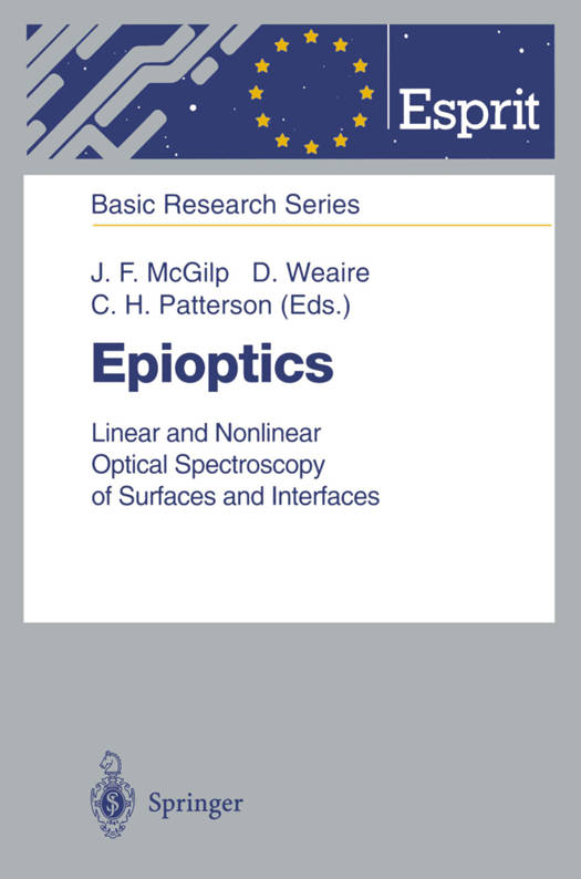
Epioptics
Linear and Nonlinear Optical Spectroscopy of Surfaces and Interfaces
€ 54,45
+ 108 punten
Omschrijving
The study of condensed matter using optical techniques, where photons act as both probe and signal, has a long history. It is only recently, however, that the extraction of surface and interface information, with submonolayer resolution, has been shown to be possible using optical techniques (where "optical" applies to electromagnetic radiation in and around the visible region of the spectrum). This book describes these "epioptic" techniques, which have now been quite widely applied to semiconductor surfaces and interfaces. Particular emphasis in the book is placed on recent studies of submonolayer growth on well-characterised semiconductor surfaces, many of which have arisen from CEC DGJGII ESPRIT Basic Research Action No. 3177 "EPIOPTIC", and CEU DGIII ESPRIT Basic Research Action No. 6878 "EASI". Techniques using other areas of the spectrum such as the infra-red region (IR spectroscopy, in its various surface configurations), and the x-ray region (surface x-ray diffraction, x-ray standing wave), are omitted. The optical techniques described use simple lamp or small laser sources and are thus, in principle, easily accessible. Epioptic probes can provide new information on solid-gas, solid-liquid and liquid-liquid interfaces. They are particularly suited to growth monitoring. Emerging process technologies for fabricating submicron and nanoscale semiconductor devices and novel multilayer materials, whether based on silicon or compound semiconductors, all require extremely precise control of growth at surfaces. In situ, non-destructive, real-time monitoring and characterisation of surfaces under growth conditions is needed for further progress. Both atomic scale resolution, and non-destructive characterisation of buried structures, are required.
Specificaties
Betrokkenen
- Uitgeverij:
Inhoud
- Aantal bladzijden:
- 230
- Taal:
- Engels
- Reeks:
Eigenschappen
- Productcode (EAN):
- 9783642798221
- Verschijningsdatum:
- 24/11/2011
- Uitvoering:
- Paperback
- Formaat:
- Trade paperback (VS)
- Afmetingen:
- 156 mm x 234 mm
- Gewicht:
- 353 g

Alleen bij Standaard Boekhandel
+ 108 punten op je klantenkaart van Standaard Boekhandel
Beoordelingen
We publiceren alleen reviews die voldoen aan de voorwaarden voor reviews. Bekijk onze voorwaarden voor reviews.


